Copyright The American Physical Society 1997. All rights reserved. Except as provided under U.S. copyright law, this work may not be reproduced, resold, distributed or modified without the express permission of The American Physical Society. The archivial version of this work was published in Phys. Rev. Lett. 78(5), 891 (February 3, 1997).
PRL online - Relevant Issue, 78(5) - This paperTo properly read some greek symbols on this page, you will need to have a Symbol font installed.
Band Mobility of Photoexcited Electrons
in Bi12SiO20
Ivan Biaggio*, Robert W. Hellwarth and Jouni P. Partanen**
University of Southern California
Departments of Physics and Electrical Engineering
Los Angeles
CA 90089-0484
(Received 10 May 1996)
We determine the band mobility of photoexcited electrons in cubic n-type
Bi12SiO20.
We measure a room temperature mobility of 3.4 ± 0.5 cm2/(Vs) that decreases
63.20.Kr, 72.20.Fr, 72.10.Di, 42.70.Nq
The mobility of a photoexcited electron drifting in the conduction band of transparent n-type cubic Bi12SiO20 crystals (n-BSO) at 300 K has been reported to lie between 3 and 5 cm2/(Vs) [1,2,3]. If the usual independent-collision model were used to describe this drift, the thermal mean free path (~ 0.2 nm) would be less then the De Broglie wavelength of the electron, and the collision rate times the Planck constant (the uncertainty in the electron energy) would be an order of magnitude greater than the thermal energy. In this "strong coupling" case the Boltzmann equation cannot be expected to apply. We report measurements of mobility vs. temperature in n-BSO which can be explained well by a "polaron" theory that avoids the limitations of the Boltzmann equation [4,5,6,7].
An electron in a polar crystal polarizes the lattice in its neighbourhood. The electron moving with its accompanying lattice distortion is called a polaron. We argue that a photoelectron in n-BSO constitutes the clearest case of a strongly coupled "large" polaron, i.e. a polaron whose wave function extends over many atoms, so that the electron can be thought of as interacting with phonons rather than with independent atoms. Previous examples of large polarons were found in a variety of alkali halides, where mobility values lie above ~12 cm2/(Vs), the values for KCl and KBr at 330°C [8]. These materials are closer to the case of independent collisions. Band mobilities lower than in n-BSO, like the value of 0.5±0.1 cm2/(Vs) found in orthorhombic KNbO3 [9], correspond to "small" polarons. Small polarons have a wavefunction extending less then an interatomic distance and move by hopping or tunneling [10]. Many even smaller mobility values are reported for various insulators, but these generally reflect the effects of shallow traps [1,11].
n-BSO has a sufficiently large linear electro-optic effect, so that charge separations can be easily seen. Therefore, we determine the electron mobility using the holographic time of flight (HTOF) method [9,11,12,13,14], in which two interfering laser beams excite a spatially sinusoidal pattern of charge carriers in the bulk of the sample. The evolution of this pattern is measured optically by observing the development of the space-charge-induced index change caused by the separation of the free carriers from their excitation point. HTOF techniques offer two distinct advantages over regular time-of-flight methods: (1) The length scale is set by the spatial period of the sinusoid and is easily varied. (2) The movement of the photoelectrons is measured optically, allowing a higher time resolution (given by the laser pulse length, which is 30 ps in our case). HTOF measurements can be performed in the presence of an applied electric field (drift mode) [13], or without any applied field (diffusion mode) [9,14], where purely thermal diffusion of the photoexcited charge distribution is measured. In this work we use the HTOF technique in diffusion mode, which has a number of additional advantages: (3) no electrodes are needed, (4) no particular sample shapes are required, and (5) no uncertainties are introduced because of possible internal electric field variations caused by trapped space-charge.
The experimental four-wave-mixing configuration is shown in Fig. 1. We use a frequency-doubled Nd:YAG laser that produces 30 ps, 532 nm pulses at a repetition rate of 5 Hz. A beam splitter sends part of a pulse into a delay line, to act as a probe beam, and the other part is split again into two write pulses that arrive simultaneously in the sample. They excite a sinusoidal electron distribution, ~sin (Kg z), from donor sites with energy levels near the middle of the 3.2 eV band gap into the conduction band. Their charge is compensated initially by that of the newly created ionized donor sites. Diffusion tends to make the conduction band electron distribution uniform, uncovering the space charge field Esc of photoionized donor sites with the following time dependence [13,14]:
 (1)
(1) where t -1 = t0-1 + tD-1. t0 is the average time for photoexcited electrons to remain in the conduction band before going to uniformly distributed traps of unknown origin. tD is the diffusion time:
 (2)
(2) Here e is the unit charge, Kg is the magnitude of the sinusoidal space-charge modulation wavevector, µ is the band mobility, k is Boltzmann's constant, and T is the absolute temperature. This analysis assumes that a small fraction of the donors are photoexcited, and that the evolution of the photoelectron pattern is dominated by diffusion, as justified experimentally below.
The space charge field of (1) modulates the refractive index of the material via the linear electro-optic (Pockels) effect. We detect the resulting phase grating by diffracting the time-delayed probe pulse from it (see Fig. 1). We note that the build-up time of the space-charge field (1) does not depend on the write fluence [14], and that it is given by the diffusion time when it is much shorter than the free carrier lifetime. We know that photoexcitation of holes is not influencing our measurement, for, if hole transport were significant, we would not observe the time dependence in (1).
The sample is homogeneously illuminated all the time by a 514 nm Argon Ion laser beam with an intensity of approximately 0.1 W/cm2. In the 0.2 s interval between two measurements, this illumination erases the space-charge induced grating created by the write pulses. During the measurement time (a few ns) the erase beam deposits six orders of magnitude less energy than the write pulses. We verified that it does not affect our results.
We use three nominally undoped n-BSO samples labelled SU1, CT1, and CT3. These crystals are well characterized by many experiments as described in Refs. 15,16. The SU1 sample has been used in previous HTOF experiments in the drift mode [2,11,13].
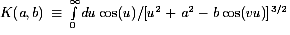
The result of a typical measurement is shown in Fig. 1. When the probe pulse precedes the write pulse there is only a small signal. A relatively strong signal caused by third order nonlinear effects is observed when the three pulses are present in the crystal at the same time. When the probe pulse is delayed (positive times in the figure), one sees the diffracted signal increase as the photoexcited electrons diffuse away from the positive ions at which they were bound, thus creating a space-charge field. The signal observed before zero-delay has amplitude E0 and is due to scattered light from the probe pulse and to the remains of a grating that is not completely erased by the Argon Laser beam (scattered light from the write pulses was taken into account separately). Although it is very small, this background grating needs to be taken into account when measuring the build-up time. We fit the detected diffraction efficiency h to h(t) ~ |Esc(t)+E0|2 by adjusting E0 and t [see (1)]. The relative phases of Esc and E0 are uncertain, especially at the low intensities where we performed the build-up time measurements. For each data set we perform two least squares fits: once imposing a phase-shift of 90° between E0 and Esc and once imposing a 0 phase shift. To obtain a final value for the rise time, we average the results of the two fits, which differ by 20% at most.
In order to determine the mobility accurately, we must establish that we are in the low-fluence limit discussed above. To do this we measure the fluence-dependence of both the build-up time and the magnitude of the signal. Fig. 2a shows the grating amplitude and the build-up time t as a function of write fluence in sample CT3. For small fluences, the grating amplitude grows linearly with the fluence of the write pulses and the build-up time is a constant independent on fluence. As the write fluence F approaches 10 mJ/cm2 saturation effects appear [9]. From the data in Fig. 2a one derives a photoexcitation cross section s between ~10-18 and 10-17 cm2, consistent with an earlier estimate [15]. We performed all the mobility measurements described below with a write fluence of the order of 1 mJ/cm2.
The dependence of the build-up times on grating spacing 2 p/Kg is shown in Fig. 2b. The data points were obtained by averaging several measurements. The build-up time is proportional to the square of the grating spacing. This confirms that the electron avoids shallow and deep traps for so long that the build-up time t corresponds to the electron diffusion time tD and the grating build-up is dominated by diffusion (see (1), t =tD). The electron lifetime t0 in the SU1-sample has been independently determined to be 26 ± 2 ns [13]. The solid line in Fig. 2b is the result of a least-square fit of (2) to the data of both samples, with only the mobility as a free parameter. It gives a mobility value of 3.4 ± 0.5 cm2/(Vs). The build-up times in the SU1 and CT3 samples are the same within the experimental error. This suggests that the mobility is an intrinsic property of the material. This idea is also supported by our measurements in the CT1 crystal at the two largest grating spacings, where we found the build-up time to agree with the results in Fig. 2b. Our mobility value is consistent with other, less accurate results reported previously [1,2,3]. A mobility of 50 cm2/(Vs) derived from grating build-up time in a similar experiment [17] is erroneous because trapping, not diffusion, dominated the dynamics [18].
Fig. 3 shows the temperature dependence of the band mobility in CT3 and SU1. The sample was enclosed in a temperature-controlled oven with small apertures for the laser beams. We set up the experiment at room temperature and selected an appropriate write fluence around 1 mJ/cm2 as described above. We raised the temperature, stopping every 20-30 degrees to stabilize it and perform a measurement. Care was taken not to change the adjustment of the experimental setup when changing the temperature of the crystal. The data in Fig. 3 was obtained at a grating spacing of 0.38 µm. Other measurements performed at longer grating spacings from 0.43 to 0.57 µm give the same temperature dependence, within experimental error.
The observed decrease of the mobility with rising temperature and the polar nature of the n-BSO lattice suggest that the band mobility is controlled by interaction with longitudinal optical (LO) phonons [4,5,6,7]. The interaction of an electron with a polarizable lattice has been studied in Refs. 5,6,7 starting from the "Fröhlich Hamiltonian" which has three material parameters: the electron-phonon coupling constant a, a single LO phonon frequency nLO, and the effective mass of the electron in the conduction band. In the alkali halide crystals where much of the polaron theory was applied [8], a single LO phonon frequency is appropriate. However, n-BSO has many polar optical vibrational branches with frequencies between 50 cm-1 and 900 cm-1 [19]. In order to apply the extensive predictions of the existing polaron models [4,5,6,7] to our results, we have devised two mathematical schemes to imitate the phonon structure in n-BSO by a single "average" or "effective" LO phonon branch having frequency nLO Hz and oscillator strength W Hz. These are related by (W2/nLO2)=einf-1 - edc-1. Here einf=5.7 is the long wavelength limit of the electronic contribution to the refractive index squared, and edc=50 is the clamped dc dielectric constant. Our schemes determine nLO and W from the experimental infrared reflectivity spectrum of n-BSO at room temperature [19]. In terms of nLO and W, the dimensionless coupling constant a defined by Fröhlich is
 (3)
(3) where Ry=13.6 eV is one Rydberg of energy, h is Planck's constant, m* is the effective mass of an electron in the conduction band (with no phonons), and me is the electron mass. Using the frequency dependence of the dielectric constant of n-BSO we obtain, from one scheme, W/c = 195 cm-1 and nLO/c = 504 cm-1, and thus a coupling constant a= 2.25 (m*/me)1/2. A second scheme gives W/c= 195 cm-1 and nLO/c = 495 cm-1 instead, which makes negligible difference in the predictions.
Since our experiment was performed above room temperature, we use the general result (Eqs. (46) and (47)) of Ref. 7, obtained before the low temperature limit was taken:
 (4)
(4)
where µ is the mobility,
b = hnLO/(k T),
 ,
,
a2=(b/2)2 +Rb coth(b v/2),
b= Rb /sinh(bb v/2),
R=(v2 - w2)/(w2 v),
and v,w are temperature dependent variational parameters
[5,6]. We find that putting b=0 in
(4) makes less than 0.1% error throughout our
temperature range. This is useful because K(a,0)=K1(a)/a, where
K1 is a modified Bessel function [20]. We note that
(4), where K1(a)/a can be substituted for K(a,b),
becomes equal to Eq. (24) in Ref. 21 in the limit
of small a.
We determined the parameters v and w at every temperature by following the free energy minimization procedure described in Ref. 6. Table 1 gives the values of the v,w parameters in the temperature range we investigated. Using these values we estimate a polaron radius of approximately 0.6 nm [22]. The n-BSO unit-cell is 1.0 nm large and contains 66 atoms. The sphere defined by the polaron radius contains ~ 60 atoms. Therefore, the continuum approximation of Refs. 5,6,7 can be applied.
The only unknown parameter in (3) and (4) is the electron effective band mass m*. The prediction of (4) at T=300 K corresponds to our room-temperature mobility value of 3.4 cm2/(Vs) when setting m*=2.01 me. From m* and (4) we can predict the temperature dependence of the mobility. The result is shown in Fig. 3 together with two other curves obtained using m*=1.7 me and m*=2.3 me. The agreement with the m*=2.0 me curve is very good. No parameter was adjusted to fit the experimental temperature dependence, which is given mostly by the effective phonon frequency nLO.
In conclusion, we have presented comparative and thermal evidence that photoelectrons in nominally undoped, n-type Bi12SiO20 are large, strongly coupled polarons; their observed band mobility is intrinsic. Their small mobility makes photoelectrons in n-type Bi12SiO20 the clearest example of such polarons.
We would like to acknowledge the support of the Air Force Office of Scientific Research under Grant No. F49620-94-1-0139.
Table 1:Variational parameters v and w for various coupling constants a and temperature parameters b.
| a=2 | a=2 | a=3 | a=3 | a=4 | a=4 | |
| v | w | v | w | v | w | |
| b=1.5 | 5.52 | 4.29 | 6.02 | 4.01 | 6.66 | 3.70 |
| b=2.0 | 4.48 | 3.40 | 4.94 | 3.16 | 5.54 | 2.88 |
| b=2.5 | 3.89 | 2.93 | 4.32 | 2.70 | 4.90 | 2.45 |
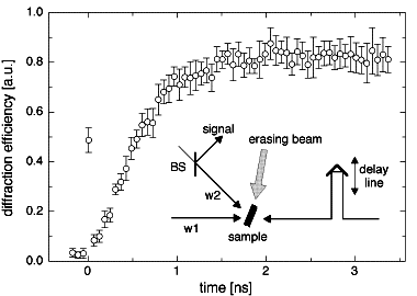
Figure 1: Diffracted signal vs. probe-pulse delay time in sample CT3,
at a grating spacing of 0.38 µm. The inset shows the experimental
arrangement. Two pulses w1 and w2 (532 nm, 30 ps) arrive in the
sample at the same time. The probe pulse, which is counterpropagating
to w1, is diffracted by the space-charge grating and produces a signal
pulse counterpropagating to w2. The beam splitter BS sends the signal
pulse into the detection system. The beam diameters are 1.7 mm for
the write beams and 0.5 mm for the probe beam. All beams are
vertically polarized. The grey arrow represents a cw erasing beam at
514 nm. It illuminates the crystal from the top with an intensity of
approximately 0.1 W/cm2.
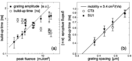
Figure 2: (a) Grating build-up time and amplitude vs. write pulse
fluence in sample CT3 for a grating spacing of 0.56 µm. The
dashed line gives a linear dependence of the grating amplitude on
fluence. (b) Log-log plot of the grating build-up time t vs.
grating spacing in samples SU1 and CT3 at 1 mJ/cm2 fluence. The
solid line is obtained from Eq. (2) using a mobility value of
3.4 cm2/(Vs).
Figure 3: Electron band mobility vs. temperature in sample SU1
and CT3, and predictions of Eq. (4).
References
* Permanent address: Nonlinear Optics Laboratory, Institute of Quantum Electronics, Swiss Federal Institute of Technology, ETH-Hönggerberg, CH-8093 Zürich.
** Also with: 3D Systems, 26081 Avenue Hall, Valencia, CA 91355.
- G. Le Saux, A. Brun, IEEE J. Quantum El. QE-23, 1680 (1987); P. Nouchi, Ph.D. Dissertation, University of Southern California, Los Angeles (1992); P. Nouchi, J.P. Partanen, R.W. Hellwarth, Phys. Rev B 47, 15581 (1992).
- P. Nouchi, J.P. Partanen, R.W. Hellwarth, in Conference on Lasers and Electro-Optics, 1992, Vol. 12, OSA Techinical Digest Series (Optical Society of America, Washington, D.C.1992), p. 84.
- S.L. Sochava, K. Buse, E. Krätzig, Phys. Rev. B 51,4684 (1994).
- H. Fröhlich, Advances in Physics 3, 325 (1954).
- R. P. Feynman, Phys. Rev. 97, 660 (1955).
- Y. Osaka, Progress of Theoretical Physics 22, 437 (1959).
- R. P. Feynman, R. W. Hellwarth, C. K. Iddings, and P. M. Plazman, Phys. Rev. 127, 1004 (1962).
- F. C. Brown, in "Point Defects in Solids", edited by J. H. Crawford and L. M. Slifkin, Plenum Press, New York-London 1972, chapter 8.
- M. Ewart, I. Biaggio, M. Zgonik, P. Günter, Phys. Rev. B 49, 5263 (1994).
- D. Emin, Physics Today 35, 34 (June 1982).
- P. Nouchi, J.P. Partanen, R.W. Hellwarth, J. Opt. Soc. Am. B 9, 1428 (1992).
- G. Pauliat, A. Viling, J.C. Launay, G. Roosen, J. Opt. Soc. Am. B 7, 1481 (1990).
- J.P. Partanen, J.M.C. Jonathan, R.W. Hellwarth, Appl. Phys. Lett. 57, 2404 (1990); J.P. Partanen, P. Nouchi, J.M.C. Jonathan, R.W. Hellwarth, Phys. Rev B 44, 1487 (1991).
- I. Biaggio, M. Zgonik, P. Günter, J. Opt. Soc. Am. 9, 1490 (1992)
- Ping Xia, J.M.C. Jonathan, J.P. Partanen, R.W. Hellwarth, Opt. Letters 18, 1780 (1993).
- F.P. Strohkendl, P. Tayebati, R.W. Hellwarth, J. Appl. Phys. 66, 6024 (1989).
- J.M.C. Jonathan, G. Roosen, and P. Roussignol, Opt. Lett. 13, 224 (1988).
- G. Pauliat, G. Roosen, J. Opt. Soc. Am. B 7, 2259 (1990).
- W. Wojdowski, T. Lukasiewicz, W. Nazarewicz, J. Zmlja, Phys. Stat. Sol. (b) 94, 649 (1979).
- M. Abramowitz, I.A. Stegun, Handbook of Mathematical Functions, Dover publications, Inc., New York, 1972.
- K. K. Thornber, R. P. Feynman, Phys. Rev. B 1, 4099 (1959).
- T. D. Schultz, Phys. Rev. 116, 526 (1959).