

Center for Photonics and Nanoelectronics

Leadership, faculty, students
Equipment, resources, expertise

Fundamentals, effects, solutions
The Center for Photonics and Nanoelectronics (CPN) at Lehigh University arose from the merger of two previous longstanding Lehigh research centers: the Center for Optical Technologies, which was devoted to photonics research, and the Sherman Fairchild Center for Solid-State Studies, which concentrated on research in electronics and solid state devices. The CPN is devoted to exploration in photonics, electronics, and solid state devices. We channel Lehigh’s intellectual and physical resources into breakthrough photonics and nanoelectronics research that serves to address hot-button challenges in energy, sustainable infrastructure and environment, and healthcare and biomedicine, to name a few.
The CPN brings together faculty members from the college of engineering and the college of arts and sciences who have relevant expertise in photonics and nanoelectronics. A core group of about 10 members is in charge of the Center’s initiatives, in collaboration with a membership of about 20 other faculty with research groups active in the photonics and nanoelectronics area.
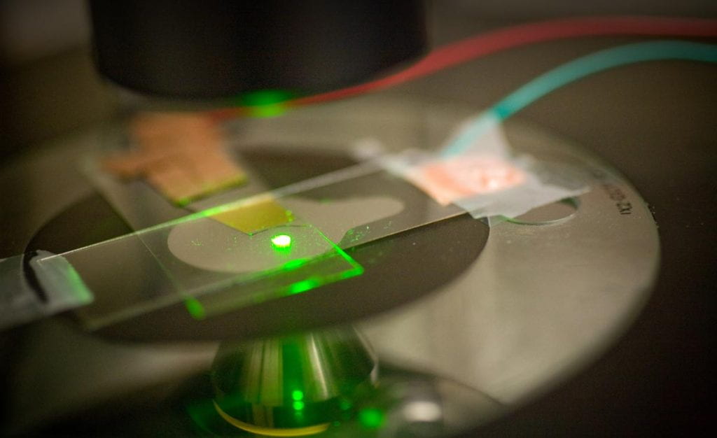
CPN’s scientific research research focuses on effects, materials, and systems that mediate the interaction between photons or allow the conversion of signals between the photonics and electronic planes. CPN’s expertise includes investigative capabilities in optoelectronics, nonlinear optics, laser spectroscopy, microscopy, and scanning probe techniques. On the materials front, activities range from individual organic molecules, organic semiconductors and polymers, to wide bandgap semiconductors, self-assembled nanostructures and two-dimensional layered materials. Current strengths span from III-Nitride and compound semiconductor technologies to terahertz sources, organic based optoelectronics and quantum photonics, nonlinear optics, glasses, bio-related materials and devices.