Copyright The American Physical Society 1997. All rights reserved. Except as provided under U.S. copyright law, this work may not be reproduced, resold, distributed or modified without the express permission of The American Physical Society. The archivial version of this work was published in Phys. Rev. Lett. 78(1), 106 (January 6, 1997).
PRL online - Relevant Issue, 78(1) - This paperNote: Because of a typing error, the words "holes" and "electrons" were exchanged when giving the mobility anisotropy for KNbO3 in the abstract of the archivial version.
To properly read some greek symbols on this page, you will need to have a Symbol font installed.
Anisotropy of the electron and hole drift mobility in KNbO3 and BaTiO3
Pietro Bernasconi, Ivan Biaggio, Marko Zgonik and Peter Günter
Nonlinear Optics Laboratory
Institute of Quantum Electronics
Swiss Federal Institute of Technology
ETH Hönggerberg, CH-8093 Zürich,Switzerland
(Received 6 September 1996)
We determine the anisotropy of the mobility of photoexcited charge carriers
71.38.+i, 72.20.Fr, 72.20.Jv, 72.40.+w, 77.84.Dy
The drift mobility of photoexcited holes in tetragonal barium titanate (BaTiO3) shows an anisotropy of about a factor of 20 between the two different crystallographic directions. A recent work [1] has pointed out that this anisotropy has the same temperature dependence as the anisotropy of the dielectric permittivity, a fact which lead to speculate upon a possible linear relation between the drift mobilities and the dielectric permittivities. Several hypotheses have been examined trying to explain these phenomena but none was completely satisfactory. The description of the charge transport by small-polaron hopping was not completely successful [1], either, although it was demonstrated that in BaTiO3 this process is dominant [2]. We now present new measurements of the anisotropy of the photoexcited charge carrier mobility in potassium niobate (KNbO3), another anisotropic polar material of the same family and with characteristics similar to those of BaTiO3.
These two materials belong to the oxygen-octahedra ferroelectrics with perovskite structure and are particularly interesting for electro-optical, non-linear optical as well as for photorefractive applications [3, 4, 5]. Although at different temperatures, both crystals have the same sequence of structural phase transitions, from the cubic to the tetragonal, orthorhombic and finally to the low temperature rhombohedric phase. In the lower symmetry phases, both crystals are ferroelectric and show a spontaneous polarization Ps associated with a weak lattice distortion. At room temperature, KNbO3 is orthorhombic (point group mm2) with the crystallographic b axis in the pseudo-cubic (010) direction, while the a and c axes lie along the pseudo-cubic (101) and (-101) directions. At room temperature, BaTiO3 has a tetragonal structure (point group 4mm) with the axes parallel to the cubic ones. In both materials the c axis is oriented parallel to Ps.
We determine the anisotropy of the mobility in the bulk of the material from the photoconductivity measured by a purely optical method. Using light energies smaller than the material band-gap, the photoconductivity is due to charge photoexcitation from energy levels introduced by impurities or intentional doping. In contrast to direct photoconductivity measurements, our results are not influenced by the quality of contacts between crystal and electrodes or by parasitic build-up of screening charges close to the electrodes themselves or by surface conductivity, all of which are particularly inconvenient effects in highly insulating materials like KNbO3 and BaTiO3.
We measure the bulk photoconductivity by detecting the decay of the space-charge electric fields generated by the photoconductivity itself. Two interfering laser beams first create a spatially sinusoidal charge carrier excitation rate which leads to a charge displacement from the brighter to the darker regions of the interference pattern. At steady state and small modulation depth of the interference pattern, this process converges to a sinusoidal charge distribution inside the impurity centers [6, 7] and the resulting DC electric space-charge field modulates the refractive index of the crystal via the linear electro-optic (Pockels) effect. The amplitude of the generated phase grating is monitored by the diffraction of a weak probe beam incident at the Bragg angle. The diffracted intensity is proportional to the square of the space-charge field amplitude [6, 8]. We study the decay of the phase grating when it is erased by a strong homogeneous illumination. By measuring the grating decay times for various orientations of the grating wavevector, we determine the anisotropy of the photoconductivity and thus of the charge mobility.
The amplitude of the space-charge field grating decays exponentially. The exponential time constant t is given by [5]
 (1)
(1) where eeff and e0 are the effective [9] and the vacuum dielectric constants, e is the unit charge, n is the density of free charge carriers with mobility µ, and kg is the modulus of the grating vector. The Debye screening wavevector k0 and the inverse diffusion length kd are two material constants which depend on the impurity concentration [5]. The density of photocarriers n(I) is responsible for the light intensity dependence of Eq. (1). This formula is valid for sinusoidal modulations of the space-charge distribution obtained by a low contrast illuminating interference pattern.
We choose the magnitude of kg to be much smaller than both k0 and kd. In this limit, the term between parentheses on the right hand side of Eq. (1) can be safely neglected. The decay time constant is then directly given by the dielectric relaxation time (eeffe0)/(eµn). Provided that the number density of photoexcited charges n(I) stays constant, we can write the following expression for angular dependence of the decay time constant:
 (2)
(2) where J is the angle between the grating wavevector and the c axis of the crystal and µ J=0/µ(J) describes the angular dependence of the mobility. In Eq. (2), an effective permittivity eeff must be used because of the sinusoidal spatial modulation of the internal electric field. In such cases, eeff is neither the one corresponding to a strain-free (clamped) crystal, nor the one corresponding to a stress-free (unclamped) crystal. The calculation of the effective dielectric constant for a particular direction of the space-charge field has to take into account the piezo-electric contributions generated by the mechanical response of the crystal to the internal sinusoidal electric space-charge field [9].
In general, the mobility can be described by a diagonal second rank tensor [10]. Although the static electric field E is always parallel to the grating wavevector, the drift current is generally not. Only the component of the current density parallel to the grating wavevector is responsible for the decay of the space-charge grating. By calculating this component for every direction of the grating wavevector, we can compute the effective scalar mobility as a function of J. The mobility ratio appearing in Eq.(2) is then given by
 (3)
(3) where the subscripts a, b and c denote the axes along which the mobility is considered.
In contrast to previous studies [1, 11] where only two extremal points were measured, we determine the full dependence of the decay times t of the space-charge grating on the angle J between kg and the c axis. We choose a very large grating period of 45 µm (kg=0.14 µm-1) in order to neglect the terms in the parentheses on the right hand side of Eq. (1). Taking into account that k0, kd>1.25 µm-1, the error introduced is less than 1%. The measurements have been performed in many different KNbO3 crystals including pure, iron doped, p and n-type samples, and in a nominally pure BaTiO3 probe. The crystals, cut with the surfaces normal to the crystallographic axes, are mounted so that they can be rotated around the surface normal bisecting the directions of the two beams which produce the grating (Iw1=0.03 W/cm2 and Iw1=0.21 W/cm2 ). These two beams and the erasing beam (Iw1=3.5 W/cm2 ) are provided by an Ar+ laser operating at 488 nm. All polarizations are always adjusted perpendicular to the c axis to reduce possible beam coupling or beam fanning effects [12]. The monitor beam (He-Ne at 633 nm, I = 0.01 W/cm2) is polarized along the c axis. While rotating the samples, we readjust all the polarizations by means of l/2 plates in order to ensure the same writing and, in particular, identical erasing conditions. In this way, n(I) remains unchanged and independent of J.
After the grating has reached the steady state, the grating decay is induced by blocking the two writing beams and by simultaneously switching on the strong erasing beam. All the decay curves measured for different J follow a single exponential function over at least ten decay time constants. We perform a least-squares fit of the angular dependence of t using Eq. (2), in which the angular dependence is governed by the single parameter µ a,b/µ c. The scaling parameter t(0) does not influence the form of the curves; e eff(J)/e effJ=0 is known [9, 13].
| Fig. 1 shows the grating decay time vs grating wavevector orientation in the BaTiO3 crystal while Figs. 2 and 3 present the results for KNbO3. The solid lines correspond to the least squares fit using Eq. (2). The agreement is remarkable. The mobility anisotropies obtained from the fits are summarized in Table 1. The measurement performed in the hole conducting BaTiO3 crystal agrees with the value obtained in Refs. 1, 11, 14. Experiments in electron conducting samples of BaTiO3 could not be performed because no suitable crystal was available. The only previous measurements in KNbO3 have been published in Ref. 15 but they are affected by a poor accuracy [16]. Since the absolute value of the drift band mobility along the c axis for the electrons in KNbO3 is µc= 0.5±0.1 cm2(Vs)-1 [17] we have µa= 0.6±0.2 cm2(Vs)-1 and µb= 1.0±0.3 cm2(Vs)-1. These values are similar to µc= 0.13±0.03 cm2(Vs)-1 and µa= 1.2±0.3 cm2(Vs)-1 found in BaTiO3 by Hall experiments [18]. Unfortunately, no data are available on the absolute hole band mobility for these two materials. |
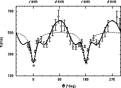
Figure 1: Decay time of the photoinduced space-charge grating in a nominally pure BaTiO3 crystal as a function of the angle between kg and the c axis of the crystal. The solid line represents the fit with Eq. (2) using e eff(J). The dashed curve is the fit obtained when using the uncorrected clamped or unclamped dielectric constants. |
Our measurements lead to several observations. The mobility ratios do not depend appreciably on the doping concentration since a concentration of the trapping centers of the order of 10-5 per unit cell can influence the charge density n(I) but not, or only to a negligible extent, the charge carrier mobility. In KNbO3, the mobility ratio µa/µc for both electrons and holes is very similar and close to unity while the ratio µb/µc shows a larger anisotropy. In BaTiO3, µa/µc is even larger.
The low mobilities observed in both materials can be understood on the basis of a small-polaron model [19]. In the one dimensional case, the small-polaron hopping mobility is of the type [20]
 (4)
(4) where a is the interatomic distance, Ea is the activation energy and J is the overlap integral of the electronic wave functions of the adjacent sites. The anisotropy of the overlap integral can be considered as the origin of the mobility anisotropy [21]. For highly localized wave functions, the overlap integral can be assumed to vary exponentially as J ~ exp(-a/r0) where r0 is the localization length. Thus, using Eq. (4) we can write
 (5)
(5) In KNbO3 the lattice constants along the a, b, and c axes are aa=5.6896 Å, ab=3.9692 Å, and ac=5.7256 Å which, combined with the mobility ratios, give a polaron localization r0 between 0.5 and 3.5 Å. These values would be compatible to the small-polaron model. However, this is not the case for BaTiO3 where the polaron localization was calculated to be 0.03 Å [1], which appears to be unphysically small.
In BaTiO3 another puzzling relation was noticed between mobility and dielectric permittivity and Mahgerefteh et al. advanced the hypothesis that the two quantities are not independent. In their work, they found µc/µa=R ec/ea where R is a constant close to 2 and temperature independent over the whole tetragonal phase. Our measurements have been carried out at room temperature but the results demonstrate that R has no universality pretence since its values in KNbO3 are close to 4 and 9 for µc/µa and µc/µb, respectively.
As already pointed out above, the solid curves in all the figures have been calculated using the effective dielectric permittivity which takes into account the piezo-electric as well as the elastic contributions in the case of a sinusoidal space-charge field. To show the importance of using the correct expression for eeff, in Fig. 1 we also plot the curve of Eq. (2) when eeff is calculated from either the clamped or the unclamped values. An evident disagreement with the measured data is obtained. Our measurement of the dielectric relaxation time as a function of the direction of the space-charge field is thus the first direct experimental confirmation of the validity of the expressions for the effective dielectric constant given in Ref. 9.
In conclusion, we have shown that optical methods can provide a reliable tool for the characterization of the charge drift mobility in photoconductive materials. The measurement of the decay time of a photoinduced space-charge fields as a function of the crystal orientation allows the precise determination of the charge carrier drift mobility ratios.
The localization length of the quasi-free charge carriers is calculated in KNbO3 according to the small-polaron model. Its value is consistent with the theory, while that obtained for BaTiO3 is too small. A further comparison of the results in BaTiO3 and in electron and hole conducting KNbO3 shows that the value which relates the mobility ratio with the corresponding dielectric permittivity ratio is a material parameter. The explanation of the temperature independence of this parameter noticed in BaTiO3, and the complete description of the charge transport mechanisms in anisotropic polar materials such as KNbO3 and especially BaTiO3, are still open questions.
We are grateful to Hermann Wüest and Michael Ewart for crystal growth and post-growth treatment and to Jaroslav Hajfler for expert preparation of KNbO3 samples. The authors also thank Germano Montemezzani for helpful comments and enlightening suggestions.
Table 1: Drift mobility ratios in single crystals of KNbO3 and BaTiO3
| Sample | Photocond. | Doping | µa/µc | µb/µv |
| KNbO3 | p type | Fe: 150 ppma | 1.05±0.06 | 2.9±0.3 |
| p type | nominally pure | - | 3.2±0.4 | |
| p type | nominally pure | - | 2.9±0.3 | |
| n type | Fe: 20 ppma | 1.15±0.09 | 1.9±0.2 | |
| BaTiO3 | p type | nominally pure | 19.6±0.6 | |
| n type | nominally pureb | 9.2±5.1c |
bReduced in flowing hydrogen [18].
cAs determined from Hall measurements in Ref. 18
Figure 1: Decay time of the photoinduced space-charge grating in a
nominally pure BaTiO3 crystal as a function of the angle between
kg and the c axis of the crystal. The solid line represents the
fit with Eq. (2) using e
eff(J). The dashed curve is the
fit obtained when using the uncorrected clamped or unclamped dielectric
constants.
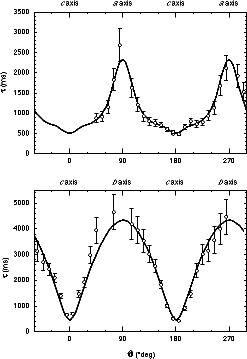 Figure 2: Decay time of the photoinduced space-charge modulation in an iron doped hole conducting KNbO3 crystal as a function of the angle between kg and the c axis of the crystal. Angular dependence in the a-c plane (above) and in the b-c plane (below). The solid line represents the fitted curve calculated from Eq. (2).
|
|
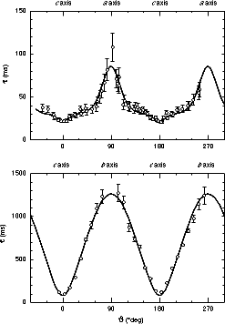 Figure 3: Decay time of the photoinduced space-charge modulation in an
iron doped electron conducting KNbO3 crystal as a function of the
angle between kg and the c axis of the crystal. Angular dependence
in the a-c plane (above) and in the b-c plane (below). The solid
line represents the fitted curve calculated from Eq. (
Figure 3: Decay time of the photoinduced space-charge modulation in an
iron doped electron conducting KNbO3 crystal as a function of the
angle between kg and the c axis of the crystal. Angular dependence
in the a-c plane (above) and in the b-c plane (below). The solid
line represents the fitted curve calculated from Eq. (
References
- D. Mahgerefteh, D. Kirillov, R.S. Cudney, G.D. Bacher, R.M. Pierce, and J. Feinberg, Phys. Rev. B 53, 7094 (1996).
- H. Ihrig, and D. Hennings, Phys. Rev. B 17, 4593 (1978), and references herein.
- M.E. Lines and A.M. Glass: Principles and applications of ferroelectrics and related materials, (Clarendon, Oxford, 1977).
- P. Günter, Phys. Rep. 93, 199 (1982).
- P. Günter and J P. Huignard eds.: Photorefractive materials and their applications I (Springer-Verlag, Berlin, 1988).
- N.V. Kukhtarev, V.B. Markov, S.G. Odulov, M.S. Soskin, and V.L. Vinetskii, Ferroelectrics 22, 949 (1979).
- G.C. Valley, and M.B. Klein, Opt. Eng. 22, 704 (1983).
- H. Kogelnik, Bell Syst. Tech. J. 48, 2909 (1969).
- M. Zgonik, R. Schlesser, I. Biaggio, E. Voit, J. Tscherry, and P. Günter, J. Appl. Phys. 74, 1287 (1993).
- J.F. Nye, Physical properties of crystals, (Clarendon, Oxford, 1957).
- C.P. Tzou, T.Y. Chang, and R.W. Hellwarth, Proc. SPIE Int. Soc. Eng. 613, 58 (1986).
- G. Montemezzani, A.A. Zozulya, L. Czaia, D Z. Anderson, M. Zgonik, and P. Günter Phys. Rev. A 52, 1791 (1995).
- M. Zgonik, P. Bernasconi, M. Duelli, R. Schlesser, P. Günter, M.H. Garrett, D. Rytz, Y. Zhu, and X. Wu Phys. Rev. B 50, 5941 (1994).
- S. Sochava, K. Buse, and E. Krätzig, Opt. Commun. 98, 265 (1993).
- S. Sochava, K. Buse, and E. Kräatzig, Opt. Commun. 105, 315 (1994).
- K. Buse, private communication (1996).
- M. Ewart, I. Biaggio, M. Zgonik, and P. Günter, Phys. Rev. B 49, 5262 (1994).
- C.N. Berglund, and W.S. Bear, Phys. Rev. 157, 358 (1967).
- D. Emin, Physics Today 35, 34 (June 1982).
- D. Emin and A.M. Kirman, Phys. Rev. B 34, 7278 (1986).
- Y.G. Girshberg, E.V. Bursian, and Y.A. Grushevsky, Ferroelectrics 6, 53 (1973).