
Welcome to the Department of Materials Science and Engineering, part of the P.C. Rossin College of Engineering and Applied Science at Lehigh University.
Accredited since 1936, the department offers one of the nation's leading materials science and engineering programs. Students work closely with award-winning professors who are at the top of their fields in a program that provides an excellent balance between theoretical and practical knowledge. | MORE >>
Department News
Zhao ’95 PhD named dean of UConn’s College of Engineering
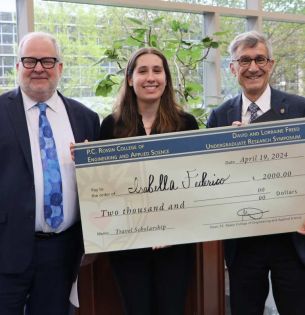
Celebrate the 2024 Undergraduate Research Symposium winners!
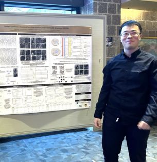
Guo brings home poster award from NECZA Meeting
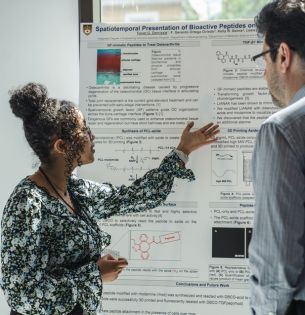
Undergraduate research takes the spotlight on April 19
Department Activity on Diversity, Equity, and Inclusion (DEI)
The Materials Science and Engineering (MSE) Department at Lehigh University is committed to diversity, equity, inclusion, and anti-racist action in our department, college, university, and beyond. We take pride in the diversity of our student body and strive to be inclusive of all members of our Lehigh community. We recognize that there is still significant progress to be made to become a truly diverse, equitable, and inclusive institution. To achieve these goals, our department is taking action as detailed on our dedicated DEI page.

